
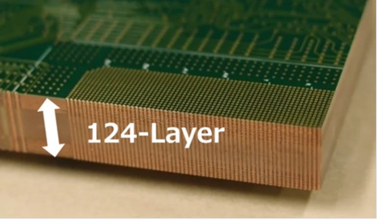
New Technology Benchmark: 124 Layer PCB from OKI Circuit
OKI’s Latest Breakthrough in PCB Density for AI Testing

Hello Friends,
Yesterday, I recorded a new podcast episode with power integrity guru Steve Sandler, which will be out later this week. During our conversation, he asked if I’d seen the news about the record-breaking 124-layer PCB. I hadn’t—but that question sent me down a fascinating rabbit hole this morning.
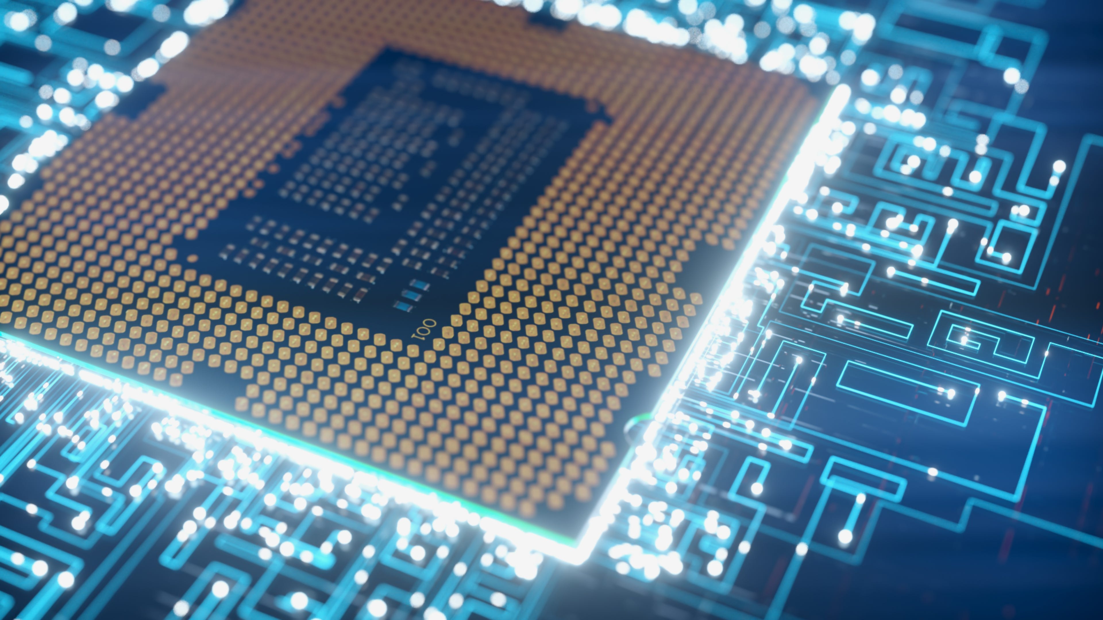
OKI Circuit Technology of Japan has officially introduced a 124-layer PCB, marking the highest known commercial stack height for semiconductor test boards to date. (The former record holder was 108 layers.) Even more impressive, they achieved this without exceeding the standard 7.6 mm board thickness (just under ⅓"), which has long been a mechanical and thermal constraint in wafer-level test systems.
This news dropped via All About Circuits in a detailed and insightful article by Luke James (May 9, 2025), and I couldn’t wait to break it down for our EEcosystem community.
Why 124 Layers Is a Big Deal
On paper, jumping from 108 to 124 layers may not sound earth-shattering. But in practice, that’s a 15% increase in routing density—achieved without compromising board thickness, reliability, or signal integrity.
Each additional layer provides critical real estate to:
Route more signals in less space
Enhance shielding
Improve management of differential pairs for bleeding-edge protocols like PCIe Gen6 and CXL 3.0
That level of density is a game-changer in wafer-level HBM testing, where vertical interconnects, power integrity, and crosstalk suppression are make-or-break factors. It’s no wonder this breakthrough caught Steve Sandler’s attention. He works closely with nearly every major semiconductor company on cutting-edge solutions—and he knows a signal integrity milestone when he sees one.
The Secret Sauce: Materials and Precision
This leap didn’t come from a single breakthrough but rather an orchestration of engineering innovations:
Ultra-thin dielectric layers just 25 µm thick
Likely use of high-performance, low-loss laminates such as Megtron 7
Symmetrical stack-ups and controlled impedance within ±5%
Thermal resilience tested through 1,000+ cycles under MIL-STD-883G
All of this while supporting:
Frequencies exceeding 112 GHz
Thermal stress endurance over 80 MPa between copper and FR-4 interfaces
This is rarefied air. We're talking AI accelerators, aerospace, defense, and next-generation telecommunications.
The Reality Check: Cost and Complexity
Of course, pushing the bleeding edge comes at a cost.
According to All About Circuits, these boards:
Cost approximately $4,800 per square meter
Require up to 16 weeks to produce
Deliver yield rates around 65% (compared to 85% for 108-layer builds)
Troubleshooting mid-stack failures often involves destructive cross-sectioning, which further impacts yield and adds complexity.
But someone has to go first.
OKI’s achievement may pave the way for broader industry adoption. The precision engineering that enables 124 layers today could help us deliver similar performance with fewer layers or smarter routing tomorrow—especially as AI-powered EDA tools and additive manufacturing continue to mature.
A Step Toward Scalable Innovation
While Denso still holds the absolute record with 129 layers (set back in 2012), OKI’s board stands out for being commercially viable, thermally reliable, and ready for production—a key distinction in a world where theoretical engineering rarely scales.
So yes, 124 layers is impressive. But the bigger story here is how this breakthrough might accelerate innovation in systems that demand more from every square millimeter of real estate.
Hope you enjoyed today’s read! Stay curious, friends!
Judy Warner
👉 Join The EEcosystem for FREE online Electronics Masterclasses from Eric Bogatin and enjoy all of our member-only benefits
Source: Luke James, “OKI Reaches New Heights With a 124-Layer PCB,” All About Circuits, May 9, 2025.
Read the full article on All About Circuits